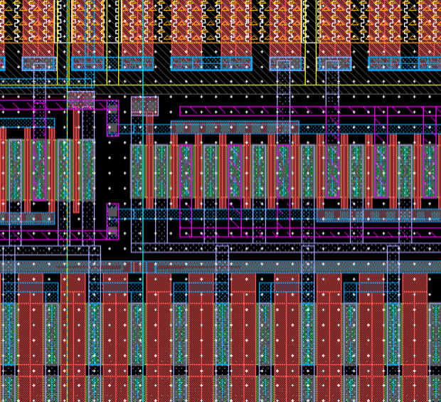
New Front-end IC with Fast Timing for Semiconductor Photodetectors
In order for the spatial and contrast resolution of PET to improve, we need PET systems with densely-packed sensors and high performance, highly integrated electronics. A PET system with small detector pixels (e.g., 1mm3 in size) results in tens-of-thousands of electronic readout channels, and this necessitates using integrated circuits (IC) for the front-end electronics. An IC is a miniaturized electronic circuit that has been fabricated on the surface of a thin piece of silicon semiconductor material. The front-end ICs currently available do not have the required dynamic range and time resolution.
We are designing a front-end mixed-signal IC with an innovative architecture that enables the analog circuits to be combined with the analog-to-digital converter (ADC) in a single IC, while consuming much less power and having a smaller electronic footprint than conventional techniques. The output of the IC will be fully digital, so it is robust against amplitude noise and pulse width jitter and also facilities multiplexing of the IC outputs. The IC will be programmable so that it can be used with both avalanche photodiode (APD) and silicon photomultiplier (SiPM) PET detectors. When completed, we are interested in sharing this IC with medical imaging researchers at other institutions so that they can use it in their data acquisition systems.
The IC will have fast timing capability, i.e., it will be able to measure the time of the pulses from the PET detectors with about 100 ps time resolution. Therefore, it could be used in time-of-flight (ToF) PET. We are targeting an analog bandwidth of 2 GHz. The size of the IC is estimated to be 1mm3 . Its small size facilitates the development of a highly compact and portable PET system form factor, which is especially important for our targeted application: breast-dedicated PET.
To design this IC, we are collaborating with the VLSI Research Group at Stanford , and we will use a design methodology that we hope will enable this project to be completed in less time and with lower risk than typical new custom IC designs in universities. This methodology, which is part of work by the Rethinking Analog Design initiative involves designing circuit blocks so they can be easily modified and re-used for other applications.