Center for Cancer Nanotechnology Excellence
and Translation (CCNE-T)
The CNSI provides an excellent environment for nanotechnology research. UCLA and University of California, Santa Barbara have joined to build the CNSI, which will facilitate a multidisciplinary approach to develop the information, biomedical, and manufacturing technologies that will dominate science and the economy in the 21st century. The 5 key elements of the CNSI's mission are to:
i) Establish a world-renowned center for nanosystems R&D
ii) Develop commercial applications of CNSI's technology
iii) Educate the next generation of scholars in nanosystems R&D
iv) Promote regional development through commercial use of nanotechnology and
v) Generate public appreciation and understanding of nanotechnology.
There is a critical need to fund scientists and engineers across disciplines and across institutional boundaries in order to push forward in the arena of nanotechnologies. There must be innovative partnerships that integrate research and education, accelerate applications, and fully explore the implications of nanotechnology on the health, wealth and lives of the American people. The vision of the CNSI is to establish a coherent and distinctive organization that serves California and national purposes and that is embedded on the UCLA and UCSB campuses. The CNSI will be a world-class intellectual and physical environment that supports collaboration among California's university, industry and national laboratory scientists.
The square footage of the CNSI building will be 184,712 square feet. It will house the following types of facilities:
i) Information Technology Infrastructure
ii) Imaging and Spectroscopy
iii) INMOS (Integrated Molecular Systems Facility)
iv) Incubator Labs
v) 4,000 sq. ft. Data Center
v) Interactive space for planning and activities
The INMOS facility refers to how UCSB and UCLA will each build user facilities designed for linking top-down semiconductor fabrication with biologically and chemically assembled molecular materials. The new facilities will complement and enhance existing infrastructure at both campuses. The current UCSB facility, part of the NSF National Nanofabrication Network, is primarily designed for compound semiconductors. The expanded facility would enable the coupling of (bio)molecular, biomimetic and mesoporous materials with NEMS. The current UCLA silicon fabrication facility will be expanded to couple silicon processing with (bio)molecules and physiologically active cells. Both campuses will focus their efforts on process development rather than just device fabrication. The square footage of the INMOS facility on the UCLA campus will be ~11,000 asf. Additionally, the CNSI will have class 100 and class 1000 clean rooms. The building completion is projected for December 2005. Project leaders Drs. Shimon Weiss (Project 5) and Anna Wu (Project 6) will have lab space in the new building (levels 3 and 5, respectively).
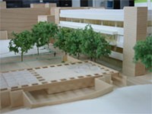
Various special considerations were made within the building; encouraging interaction between researchers across disciplines was the primary driver of the building design. Some of the elements supporting this dialog are: 6 central conference rooms; indoor and outdoor interactive spaces; hallways of interactive space that will have white boards and plenty of seating overlooking the Court of Sciences; exhibition space on a ground floor lobby; outer terraces; 260 seat theater; open labs. Floors 5 and 7 have open lab plans, which means that 3-4 labs will be in the same room. This layout will encourage cross-pollination of research discoveries.